ESR Meter
ESR Meter - Motivation

This is an ESR Meter project which I did in Mar 2022. In my many years as a electronics design engineer, I never needed a ESR meter. But recently when I was doing some repair work, I realised that I needed a tool to identify bad electrolytic capacitors. In design work, I always use new capacitor so there wasn't a need for this tool. So, I decided I should have this tool. But when I checked the price, I found that it cost too much to buy this tool. The next possibility was to make it. I know I could make this but where do I start to begin with. I decided I should just look at all the DIY designs and see which is the best I could adopt as my initial design to start with.
Let me try to share what I know, and it is always good to understand the concept before looking at details.
Concept
A ESR meter basically is an AC resistance meter. A typical multimeter measures resistance with DC. The difference with using AC is that it is able to measure the series resistance of capacitance or more technically called the Equivalent Series Resistance (ESR). A capacitor can be represented as follows

ESR is the resistance represented as a series resistor with the capacitor C.
Why do you need AC instead of DC? Since only the ESR is of interest, the capacitance has to be shorted, and this is done by using AC of a high frequency so that the capacitive reactance is very low since Xc = 1/(2*Pi*F*C) where F = frequency and C is the capacitance. When the capacitive reactance is small, the impedance measure will mostly be the ESR.
The AC used is generally in the range of 50Khz to 100Khz, square wave or sine wave does not really matter.
Design Evaluation
I have reviewed many DIY designs but I particularly like the design by Ludens because it is simple and conceptually sound.
https://ludens.cl/Electron/esr/esr.html
 Schematic 1
1. Oscillator - Using Op Amp U1A as a relaxation oscillator to generate 50Khz
2. Impedance transformation with T1 with a 20:1 ratio. This basically transforms the reflected impedance of R5 // R6 of 5 ohms to 20*20*5 = 2000 ohms which the op amp will be able to drive. Quite a simple but smart concept to solve the impedance matching issue to have maximum power transfer,
3. Amplifier gain with U1B of 39 to amplify the signal (~Vs/20 p-p)
4. AC to DC conversion with voltage doubler (using C6, D1, D2, C7)
5. Finally using a ammeter M1 as a voltmeter with R11 in series
Problem with the design
Luden's design above presents some basic design issue
1. Voltage supply - With op amp TL062, if look at the allow swing for input and output, with supply at +/-15V

Input is allowed -12 to 15 typical, but guaranteed at +/-11V
Output is allowed +/- 13.5V, but guaranteed at +/-10V
This means that the minimum voltage supply must be at least +/-5V, for very low swing of mV range. To have any meaningful swing, the voltage supply will have to be 5+Swing voltage. So if you want a swing of 2V peak, you need at least 7V, meaning 4Vp-p swing will require +/-7V (or 14V rail to rail). Clearly 7V is insufficient, and 15V is barely enough for 2.5V swing (guaranteed swing).
2. Gain of U18
The design has a inverting gain of 39. There are 2 problem with this gain.
a. With a relaxation oscillation passing through the transformer, the signal at the output assuming low loss transformation will be Vs/20. Assumming we use 15V, so the rail voltage is 15/2 = 7.5V. Then the signal will be 7.5/20 = 375mV. If the gain is at 39, then the output of U1B must be 39*0.375 = 14.625V. This clearly exceeds the rail voltage of 7.5V, which means output is distorted with flatten output max a 7.5V (if the op amp can even reach that). But as I said earlier the guaranteed output is at is 2.5V max.
b. Looking at the gain-bandwidth product for TL062 is 1Mhz, with a gain of 50, the max frequency to pass through with unity gain is 1000/50 = 20Khz. How is it possible to amplify a 50Khz signal when the gain = 1 at 20Khz?
Clearly, the amplifier gain is not correctly designed to achieve the result.
3. Metering
The conversion of the AC to DC uses a voltage doubler. If the signal is already so high, why is a doubler needed? Is it that there is a high level of attenuation in the earlier stage that make it necessary to use a voltage doubler. If we are able to create a swing in the amplifer to the max of 2.5V in the prior stage, then there is no necessity to use a doubler, a single diode detector will work as well. Finally, the meter is not buffered, which will cause voltage droop error which will get worst if a less sensitive meter is used. Even with 50uA meter the droop error could easily be signifcantly high and will get worst with a less sensitive meter.
What is suspect.
I suspect that there is loading causing a significant drop of voltage when the measurement is done, because there is insufficient drive to support it (even with transformer). This resulted in later gain stage to be increased, but suffer bandwidth reduction, so yet again voltage doubling to get the metering result. What this means it that there is a lot of errors being introduced when measuring low resistance to higher resistance, because the internal parameter are changing with the load.
New Design
The new design started with several objectives
a) To solve all the issues mentioned above.
b) To achieve the performance like a industrial product and yet low cost
c) Impose design to no more than 4 Op Amps, uses off the shelf parts, and parts that are easily available.
d) There are specific constrains which I imposed on the design to make it very low cost with easy to find parts
1) For example, I could easily find a cheap multimeter with 500uA movement instead of using a dedicated 50uA meter
2) Using a transformer from a AC-DC SMPS (like 230 to 5V USB supply) instead of a specially wound 20:1 transformer.
With the above consideration, the final design is created progressively. I said progressively, because this was not done in one go, but after several iterations of issues and resolutions from understanding the flaws of the original design.
The final design was done with the following change
1. Change the IC to TL082. This is a needed change to ensure that the swing requirement can be extended, and the bandwidth can be wider. It is not the best, but definitely better than TL062. There are at least 2 reasons for TL082. 1. It has large gain-BW product of 4Mhz. It also has a wider swing allowed which mean a lower Vs can be use. I use 12V (Vs = 6V) and max output swing is 6-3 = 3V guaranteed. Actually, I am already pushing a little beyond the quaranteed but defintely within the typical limit since the amp is having a swing of about 3.5V with a separation of 2.5V from Vs.

2. Raised the operating frequency to 70Khz which is better than 50Khz, I did try to push it to 100Khz, but the performance suffer slightly because it is already hitting the bandwidth limit of the op amp, so it does not offer much gain. I think it does not make much difference at 70Khz, since the significant square wave harmonics will be more than 200Khz.
3. I did not use a 20:1 ferrite transformer because I do not have the tools to wind one, so the easiest I can find one is a flyback transformer which is about 10:1. With that, I expect the voltage at the output to be higher at Vs/10.
4. The output need to have a strong drive to avoid loading loss which will definitely happen if it is driven directly with the op amp. Therefore a push-pull stage in included to have a low impedance drive.
5. Since I can be sure that the output loading loss is minimal, I will need only a gain of 10 to restore the signal at the test point back to the level of the oscillator without causing over drive distortion. Any loading loss will only cause the signal level to drop lower that the oscillator level, so it will always be safe to use a gain of 10 (same as the transformer 10:1)
6. To ensure that the AC-DC conversion does not suffer from loading droop due to the meter, a buffered output is created with another op amp.
7. If a gain of 10 is use, we know that the output swing is already at the max swing possible, then it makes no sense to use a voltage doubler as a AC-DC conversion. A simple single diode peak detector will be better since we know that the max output will be one diode forward voltage less, meaning the maximum swing can never be exceeded. One other compelling reason why I use a buffer is because I am using a less sensitive meter of 500uA full scale deflection which will definitely cause bad loading without a buffer. With a buffer, even a 2mA FSD meter is no problem at all.
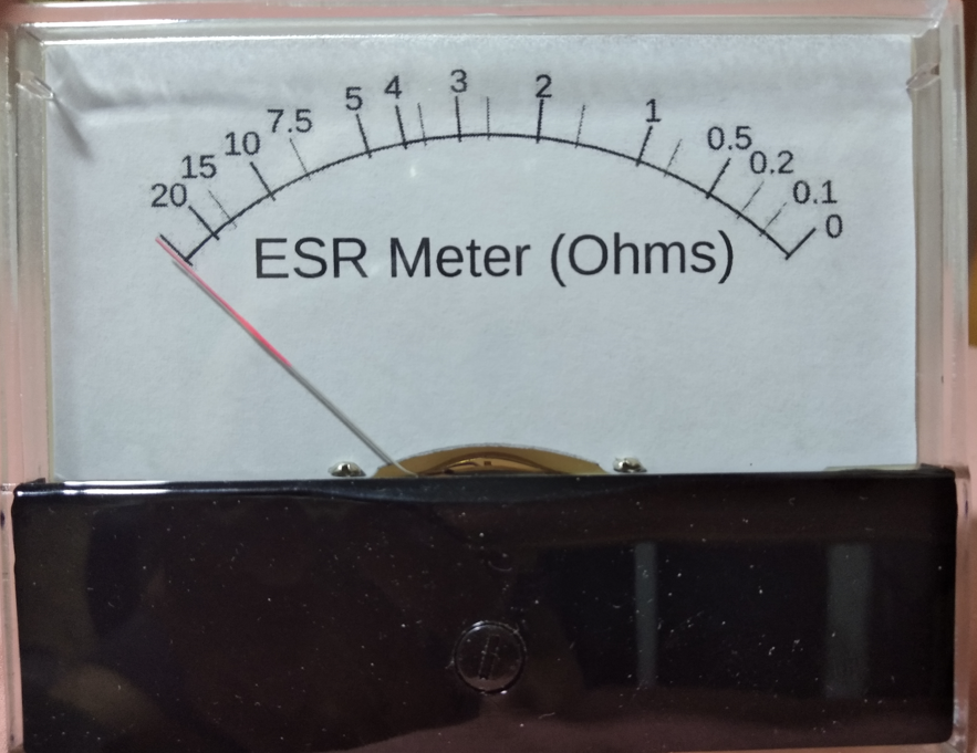
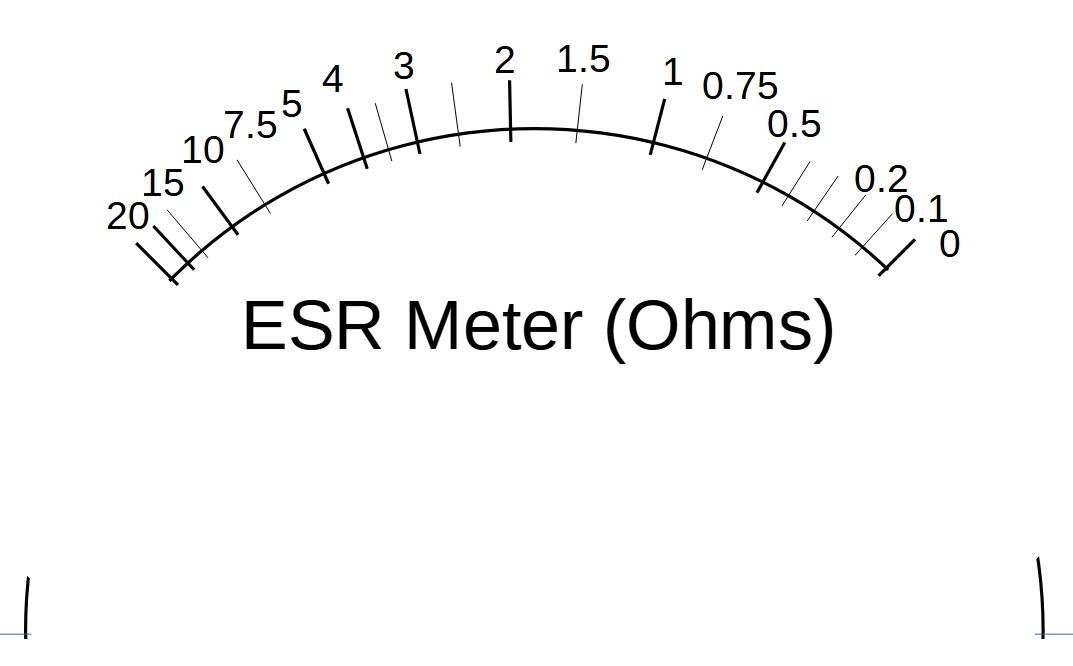
8. I change the original R6 from 10 ohm to 5 ohms, because I wanted a mid scale of the meter to be at 5 ohms instead of 10 ohms in the original design. Even though it appears that the mid scale should be at 5 ohms, it is not, because of the losses due to the reflected impedance and the resistance in the coil winding, but the error is relatively small. Actual mid scale tested with 5 ohm without correction is at 47.8% which should be relatively easy to correct to 50%.
Schematic of the final design.

10. There is one last imperfection, which is quite obvious from the scope. There is a crossover distortion because of the use of the class-B amplifier driver without crossover distortion correction. However, I will leave it as it is because I am using a square wave, so this distortion is not serious enough to affect the measurement result. In fact, after the amplifier stage, the crossover distortion disappears totally for obvious reason. The amplifier at gain of 10 is already acting as a filter to remove all the high frequency harmonics cause by the crossover distortion. I also can observe that the square wave after amplification is slight rounded at corners, which confirms my suspicion that the op amp is already operating to its limit frequency.
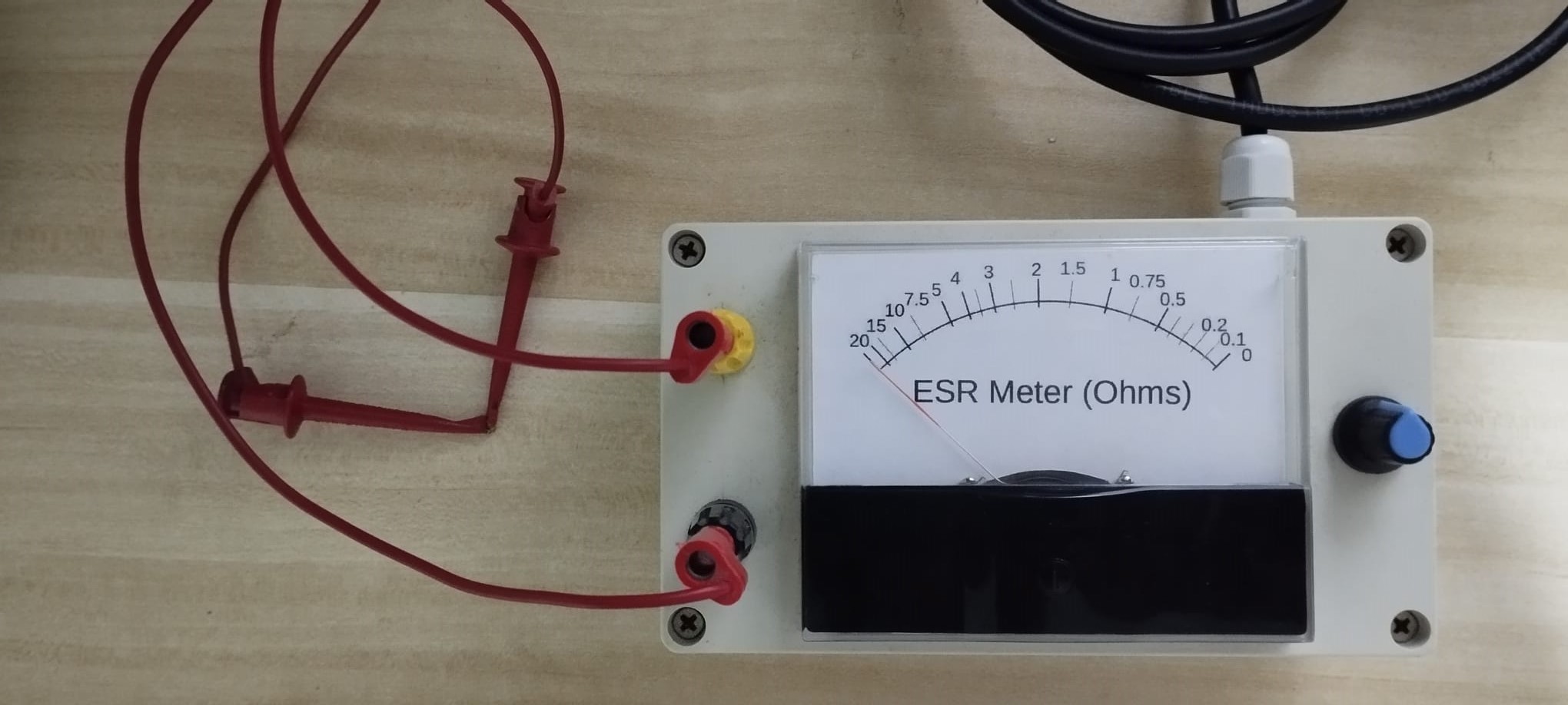
Final Product
Sorry, every small components used are SMD, so only the transformer and IC are visible


The schematics also shows the actual test value which has a progressive increasing error with respect to the expected actual under idea condition. The error is monolithic and effectively spreads the lower resistance range is more widely compared to the higher resistance range on the meter scale. The error behaviour is working in our favour since we are more interested in the lower value range, when measuring ESR.
Design Update
After posting the design, I received feedback that there is already a design by Jay_Diddy_B (5 transistor ESR meter). I reviewed the design. Indeed it is a great design using simple and cheap components to achieve the desired performance. I have even received some nasty feedback that the transformer is not needed. After looking at the design, I did some test and found that the transformer can be eliminated as long as the driver is there.
I wanted a simple to assemble design which will be easier with op amp than using transistors. Another requirement is to allow for the use of ammeter of higher full scale deflection (any meter up to 5mA should not be a problem)
The updated design is functionally similar to the 5 transistor by Jay_Diddy_B except for the AC to DC conversion. I use a simpler diode peak detector which has a range more suitable for op amp design instead of a voltage doubler design. Also the meter is now buffered so the loading of the meter is no longer a concern. The mid scale is about 2 ohms.


With Waveform


Questions to think about
1. Should you use square wave or sine wave for the oscillation?
2. How do I set the mid scale deflection to a different value?
3. What are the AC to DC conversion techniques and which is the best for this application (given the imposed constrains)?
4. What modifications are needed, if I want to operate from a 9V battery (with a least 7V)?
5. Where was the error in the reading introduced and how can we have a design with smaller error?
Note, some of the questions are already answered in the trade-off evaluations.

Hi ,no body has comented your work and modification you've made.
ReplyDeleteI can Say It was a a great guide for me.
I had mede Ludens circuito It also works great buy i wanted ti test your mods.
Your firs circuito works well aslso for me.
The only akward thing Is i dint have 50ua . I got 1of 1ma other of 2ma and that One of the economic ciness Meter yt1000.
For that One of One ma i change the 5ohm to a trimer to change the rage of scale. And the One R11 i change It for One of 1.3k that way arrive mor current t and voltage to the 1ma Meter.
I Power the IC with 9 V
Asimetric of that Is the word. +9v -9v and gronwd virtuale as your circuito.
Dint use 12v cause dont have +12 -12 Power suply . I use batery 9v with a Power supply.
I continuo
R11 will have to be lowered for 1mA as you have done. You can use 9V battery, it will work too.
DeleteAs i dont have tl082 i only have tl074 buy It Is working find only the signal Is not a Square It got a peak at the beginig.
ReplyDeleteAs diode of shoky i use germanium a34.
The output of the lead where i measire the esr capacitor Is 200mv RMS e 540mv PP.
-modifying R11 i can let to pass mor voltage o current depende on the ammeter.
Good work. I apreciate you job.
Good ESR
TL074 is usable too. I happen to have TL082. You can lower the test point voltage by changing the gain. I have actually modified mine to less than 180mVp-p. I will update the circuit later.
ReplyDeleteI have now modified to 260mVp-p on the test point to remove the over sensitivity of the test points for zeroing. 260mV is not overly high since shockley diode only start conduction at above 200mV which is only at the tail end of the scale which will not affect detecting a bad capacitor.
ReplyDeleteHello, first of all thank you for your detailed work here. I needed such a circuit so I've assembled it following the final schematic. I've replaced the peak detector section with an opamp based precision rectifier and the circuit behaves perfectly. How exactly were you planning to integrate the DC short detection with Q3? Thanks
ReplyDeleteThank you OrbitalVKL for trying out the design. I have no plan yet for the DC short circuit detection, though part of the circuit is there. The reason is that I will need to switch to applying DC instead of the square wave signal to the wheatstone bridge. This also means that C5 and C6 needs to be shorted. This will require additional circuit to provide this bypass. Do you have a simpler idea to detect the DC short? Another comment about using the precision rectifier, is that the OA goes into saturation when the diode is reversed bias, which leads to artifact in the response. You need to choose OA that can get out of saturation fast otherwise the reading of the rectification is not accurate. That is the reason, I chose a direct diode detection which does not give this artifact.
ReplyDeleteThanks about the extra information.
ReplyDeleteYes I've actually implemented the DC short feature and validated it's operation. I'm injecting DC at DUT+ terminal. From the same point I'm sending this voltage to an OP amp comparing it to a reference voltage I can precisely set. If there is a DC path, it will shunt the 2.2R bridge's bottom resistor. The idea is that I can measure any equivalent DC resistance from 0R to 2.2R against the 2.2R bottom resistor of the bridge. The OP then drives an LED. Calibration is done using a variable resistor as a DUT. As I've extended the device capabilities (with a capacitor discharge section and a signature curve tracer section), the power supply had to be redesigned with a true +/-15V rail. I'm feeding the system from a 18650 cell (floating device) through a BMS, a boost converter and a 12V to +/-15V DC-DC converter. I'm now close to final design. I can provide schematics if you wish.
Regards.
How about the DC blocking capacitor at the input of the differential amp. Do you short these capacitors during the DC measurement or you totally remove them in your design. You can remove them, but you may risk a direct blow to the Op Amp if the measured cap is charged. I would like to review your design when done.
ReplyDeleteThis comment has been removed by the author.
ReplyDeleteThe DC test is performed in parallel of the ESR test without disturbing it as the caps are like open circuit in regard to the injected DC voltage.
ReplyDeleteWhen simulating a shorted component, the ESR meter reads low ESR (needle pointing 0) but also light up the LED. When testing a very low ESR, needle is close to 0 but the LED stays off. I forgot to mention that the path leading to the DC short comparator OA (different from the ESR OA) is fitted with a low path filter so parallel operation is possible.
I think I understand, so basically you are applying DC + AC on the signal injection. By measuring the mean DC level before the capacitors connecting the differential amp you determine the short at the test terminal. That is a possible strategy. Will be interesting to see your design. The AC level must be trimmed down a little to allow for some DC offset without causing saturation, because the current design of the oscillator is using the full swing of the supply in the AC (square wave) which does not allow for DC offset.
ReplyDeleteIn addition, you need a simple low pass filter to remove the AC component when measuring the DC.
ReplyDeleteYes you got it right. I've also implemented the low pass filter. The only remaining issue now is probably linked to the oscillator section as you said. By switching from virtual ground topology to symmetrical supply I've introduced a new problem, which is that I can't bring the needle down to infinite resistance (full left). I still need to figure out why. My breadboard setup may also bring some unexpected troubles. If you have an email I can share the schematics if you want to see the current design
ReplyDeleteThis comment has been removed by the author.
ReplyDeleteDone
DeleteHello, thank you for the design, i built your latest design and it has worked perfectly. Im planning to do my bachelors thesis based on your design with some changes, if that's ok with you. Also if Orbital is also reading this, can you share your dc det schematic so i can also include that too on the thesis if thats ok with him.
ReplyDeleteHi Sami, please go ahead and use the design and also share what you have learnt and change so that everyone reading this blog will benefit.
ReplyDeleteHi Sami, please provide me your email here. OrbitalVKL has given me permission to sent his design to you.
ReplyDeleteThis comment has been removed by a blog administrator.
Delete